Consorzio Interuniversitario per lo sviluppo dei Sistemi a Grande Interfase
Center for Colloid and Surface Science

Optical microscopy

Reichert Zetopan

Reichert Zetopan works in reflectance and transmission mode with polarizers and interferential contrast according to Nomarski with digital camera Nikon, model . Objectives 5.5x, 11x, 28x, 56x.

Wild M5A

Wild M5A works in reflectance mode with high focal length allowing to easily manipulate the samples. Objectives 6x, 12x, 25x, 50x.

Contact Angle Microscope KSV CAM 200

Contact angle microscope and tensiometer. Suitable for sessile drop, pendant drop and captive bubble measurements. 

Confocal microscopy

Laser Scanning Confocal Microscope Leica TCS SP2

Laser Scanning Confocal Microscope Leica TCS SP2 equipped with a ISS FCS module, with 4 lasers, providing eight available laser lines. The confocal microscope is equipped with three spectral detectors for fluorescence (PMT) suitable for imaging (and z-stack), spatially resolved emission, spatially resolved FRET, FRAP and a transmission PMT. The FCS module is equipped with two APD, suitable for FCS and FCCS experiments.

Laser Scanning Confocal Microscope Leica TCS SP8

Laser Scanning Confocal Microscope Leica TCS SP8 with a DMI8 microscope with a Picoquant FCS module, with 4 lasers, providing eight available laser lines. It is equipped with one external PMT for transmission and five internal spectral detectors two PMT, one Hybrid and two cooled Hybrid detectors for Single Molecule Detection, suitable for imaging (and z-stack), spatially resolved emission, spatially resolved FRET, FRAP, FCS and FCCS. The microscope table is motorised both in z and in xy, allowing the mapping of extended samples.

Electron microscopy

Zeiss Sigma FE-SEM

Zeiss Sigma model, equipped with GEMINI column and In-Lens detector, capable of providing high resolution images on both conductive and non conductive samples. The microscope is also equipped with an X-ray detector (EDS) and a backscattered (BSE) and secondary (SE) electron detector. The Oxford Instruments INCA X-ray Detection System, in addition to conventional X-ray analysis capabilities, produces high-resolution element distribution maps.

Leica Cambridge Stereoscan S360

The Scanning Electron Microscope (SEM) is one of the most versatile and widely used tools of modern science as it allows the study of both morphology and composition of all kind of materials. High-resolution images of the morphology of a specimen, with great depth of field, at very high magnifications can be obtained. Compositional analysis of a material may also be obtained by monitoring secondary X-rays produced by the electron-specimen interaction. Characterisation of fine particulate matter in terms of size, shape, and distribution may be performed. The sample preparation is relatively easy since SEM only require the sample to be conductive. Specimens must be coated with a very thin layer of conductive material. CSGI has a Agar auto gold sputter system and as Agar auto carbon (graphite) coater.

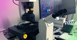
Transmission Electron Microscopy with Scanning Mode (S/TEM)

The JEOL JEM-F200 is a 200 kV TEM machine with scanning capabilities (S/TEM) equipped with a range of imaging detectors:

  •     Bright Field;
  •     High Angle Annular Dark Field;
  •     Secondary Electrons;
  •     Back-Scattered Electrons.

The electron source is a Cold Filed Emission Gun which provides:

  •     an electron beam energy spread ≤ 0.3 eV (FWHM) @ 200 kV;
  •     a brightness ≥ 8e8 A/cm2sr @ spot size = 0.7 nm;
  •     a probe current ≥ 2.5 nA @ spot size = 0.7 nm, in conjunction with the 4-lense illumination system.

The point resolution is ≤0.23 nm in conventional TEM mode and ≤0.16 nm in STEM mode, using the HAADF detector, with still the capability to tilt the sample up to angles ≥ 80°, which will allow the implementation of tomographic techniques in future

The microscope is equipped with an EDS system with analytical resolution ≤ 133 eV @ 5.6 keV ; the100 mm2 active area assures a collection angle ≥ 1 sr, which, given also the probe current values, allows fast acquisition of EDS spectra and X maps even at the high spatial resolution corresponding to small probe sizes. This instrument enables extended experiments for a wide variety of applications allowing morphological, structural and chemical nanoscale investigations.

FE-SEM Zeiss Ʃigma|VP

FE-SEM Zeiss Ʃigma|VP. The (filed emission) scanning electron microscope Zeiss Ʃigma|VP is provided with a range of imaging detectors:

  •     conventional Everhart-Thornley detector for Secondary Electrons, with high collection efficiency;
  •     4-sector semiconductor detector for Back-Scattered Electrons
  •     high-resolution in lens detector for Secondary Electrons, which (together with the electron source and the column design) allows a nominal resolution down to 1.5 nm @ 15kV

The electron source is a Thermal Field Emission Gun (a Schottky emitter). The electron-optical column is a GEMINI design and the instrument can work in Variable-Pressure (VP) mode, with pressures adjustable from 1 to 133 Pa, avoiding the need to coat non-conductive samples.

The machine is also equipped with a Bruker Quantax 200, an EDS system of the SDD type, with a 30 mm2 window which allows fast spectra and X maps acquisition; analytical resolution ≤127 eV @ 5.6 keV.

SEM Jeol JSM-5600LV

The scanning electron microscope Jeol JSM-5600LV is a workhorse with

  •     Everhart-Thornley detector for Secondary Electrons;
  •     5-sector semiconductor detector for Back-Scattered Electrons (BSE).

with resolution ≤3.5 nm @ 30 kV with Secondary Electrons

The instrument is a Variable Pressure SEM (VP-SEM); the specimen chamber pressure can be adjusted from 10 to 270 Pa. The resolution in VP mode is  ≤ 5 nm with BSE. This microscope is also equipped with an EDS system Oxford Instruments Isis Series 300, with a Si (Li) detector and a 10 mm2 window, having analytical resolution ≤133 eV @ 5.6 keV

Both the instruments allow to investigate the composition, the morphology and size distributions not only in vacuum but also in VP mode, enlarging the fields of applications. Ceramic, metal, glassy and polymeric samples are some of the materials that can be studied. Chemical mapping is possible by means of EDS. Elemental standards are also available.

Zeiss Evo MA10 SEM

The instrument allows to work both under high vacuum and in ambiental mode, for the analysis of chemical and biological samples. 

Other